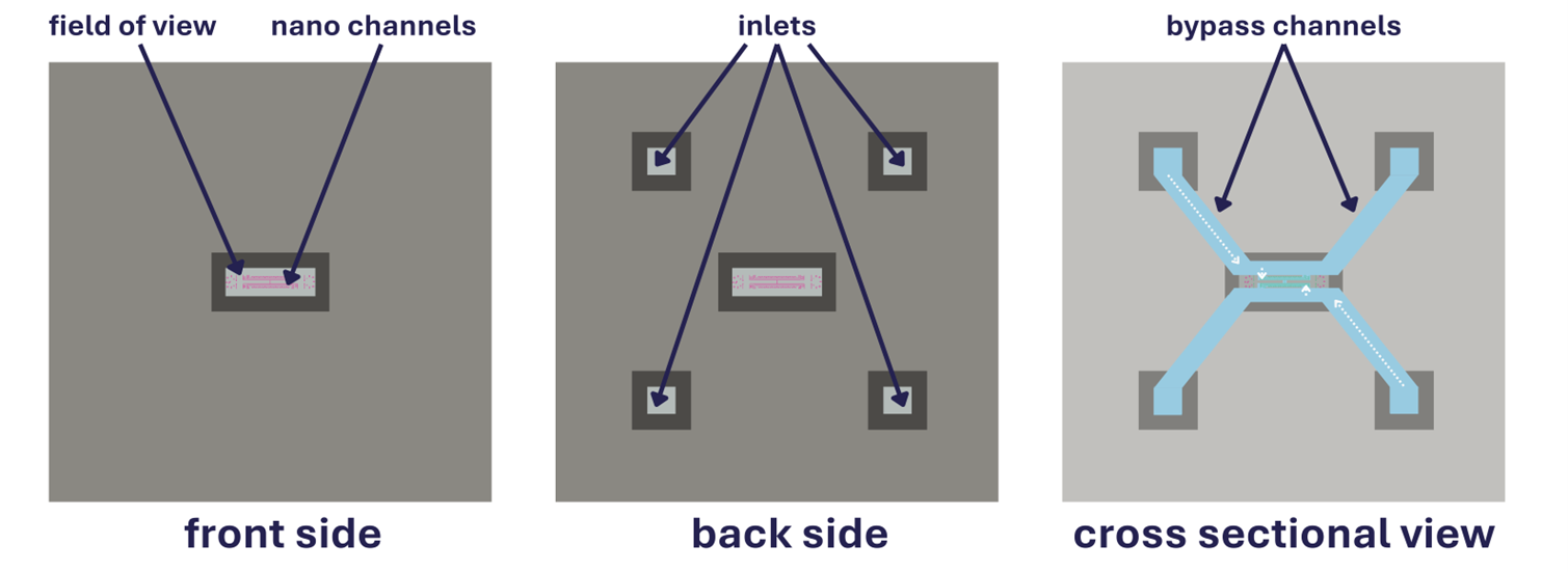
This experiment explores how silica nanospheres can be observed in a water environment using Insight Chips’ Nano Channel Chips using an SEM. These chips feature different nano channel designs that enable direct imaging of particles suspended in liquid. The channels are fabricated using very thin electron-transparent silicon nitride membrane. Silica nanospheres were chosen as a model system because their low atomic number produces weaker BSE contrast than heavy elements such as gold, making them a challenging and informative test case.
Showcase the observability and investigate the imaging challenges of silica nanospheres in a water environment at different concentrations using SEM with our Nano Channel Chips.
To separate the particles from the solvent, the original solution was centrifuged for 12 minutes in two Eppendorf tubes, each containing 0.5 mL of solution. Afterwards, the clear solvent was removed by aspirating with a pipette positioned above the concentrated sediment at the bottom. From the first tube, 0.25 mL was removed which up-concentrated the solution two times. From the second tube, 0.40 mL was removed which up-concentrated the solution five times. The obtained solutions were first mixed manually and then in an ultrasonic bath. The final concentrations corresponded to 20 mg/mL and 50 mg/mL, respectively.
The selected chips were first examined under an optical microscope to check for possible damage or contamination. To prepare the chip for drop-casting, the protective silicon nitride membrane on the inlets was punctured using an IV needle (see Figure 4). Since the membrane is very thin, a gentle poke of the needle is sufficient to puncture it, provided it is directed at the centre of the inlets.
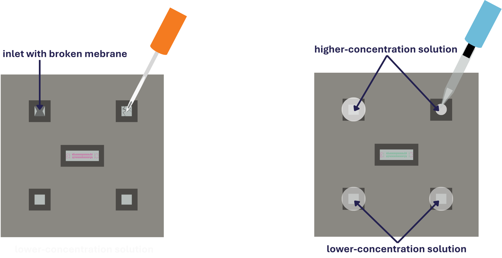
The optical microscope was then used again to verify that the membranes were punctured correctly. Once the chip was prepared, 2 μL of solution was pipetted from the Eppendorf tube and drop-cast into the inlet. In this case, the higher-concentration solution was drop-cast into two inlets on the upper side, and the lower-concentration solution into two inlets on the lower side. The liquid was drawn into the nano channels almost immediately by capillary force.
After drop-casting, the chips were again examined under the optical microscope. The presence of liquid inside the nanochannels was confirmed by a color change and by comparison with empty navigation channels.

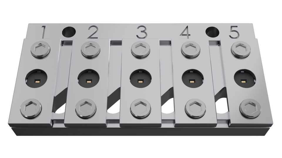
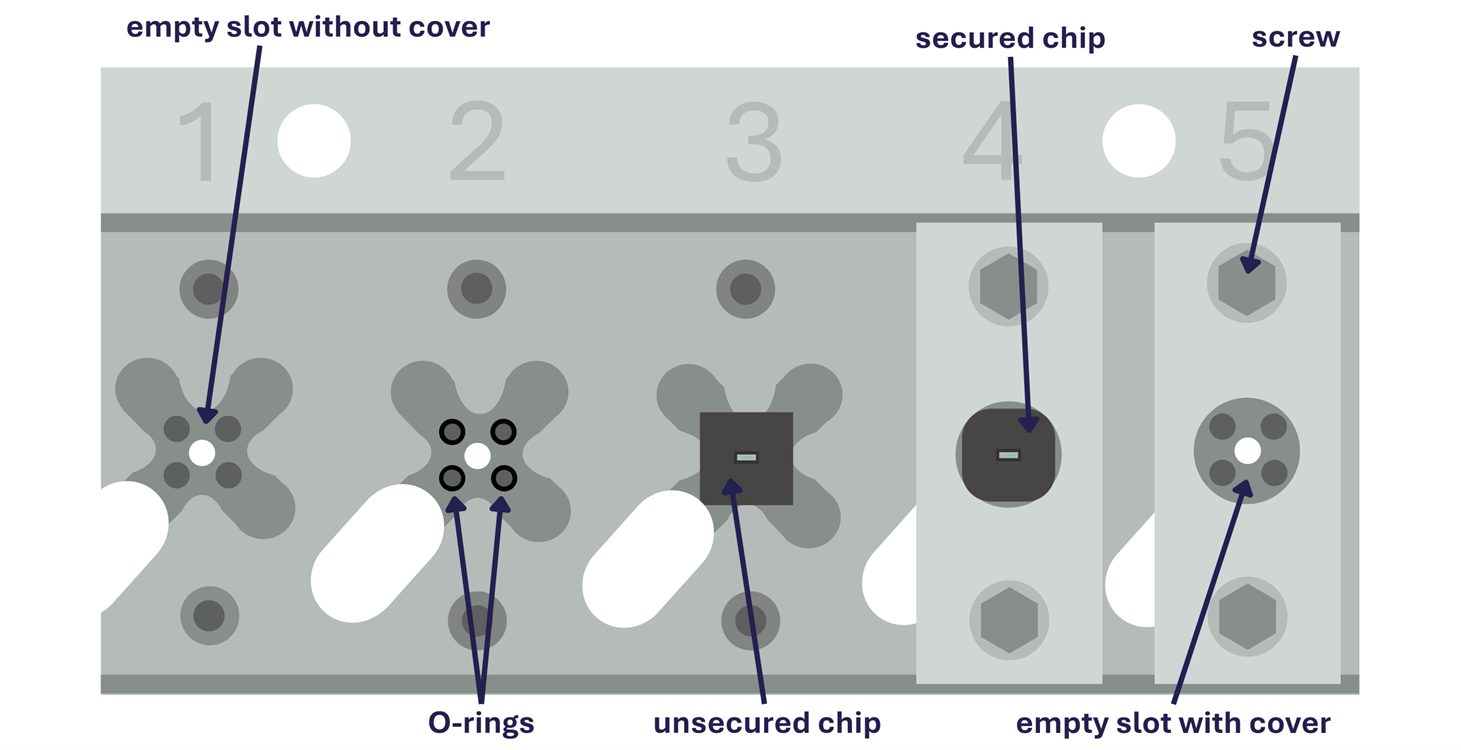
In the final step, the chips were inserted into the static SEM holder with the inlets facing downward, so that the O-rings previously placed on the holder sealed the liquid inside. The chips were then secured with a metal cover lid tightened by screws.
The SEM holder was inserted into the microscope with the aid of an elevated pin stub holder and secured onto the large stub using carbon tape.
During imaging, it was necessary to minimize the electron dose per unit area, as electron beam exposure induces movement of the particles and liquid, which can result in channels drying out, mainly due to radiolysis of water, heating, and charging of insulating materials. An appropriate combination of low accelerating voltage, higher scanning speed, and larger pixel size helped to reduce this movement and improve image quality. In this study, the beam current was set to 0.80 nA, with scanning speeds of 1, 3, and 5 μs per pixel and pixel widths ranging from 564 pm upward.
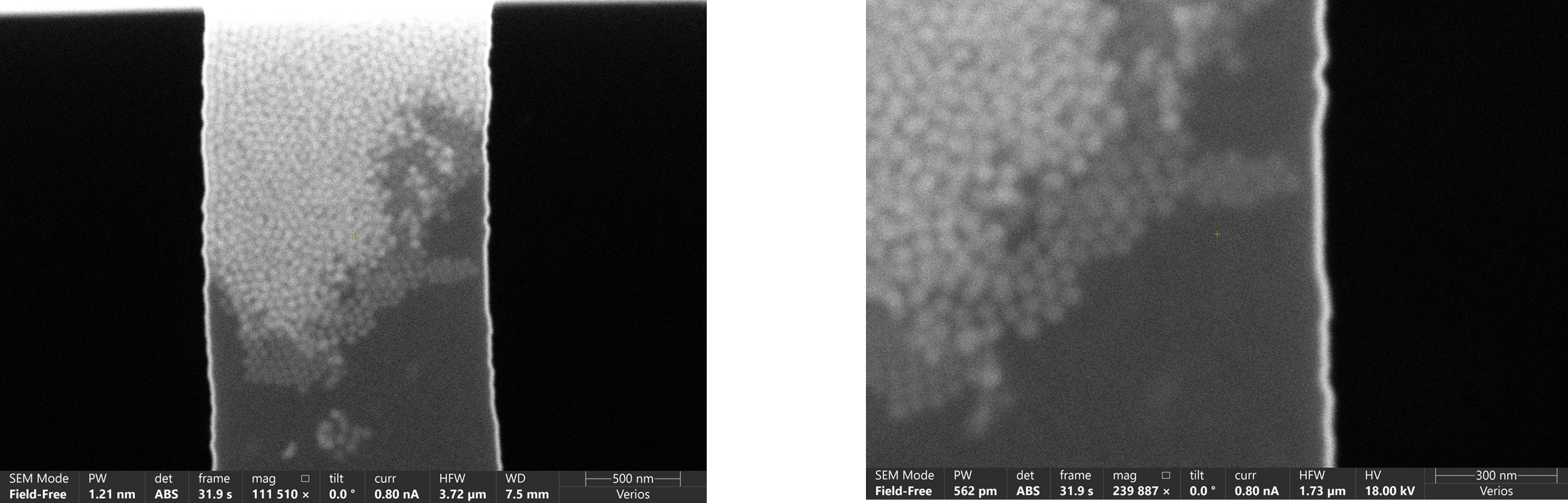
A good practice for achieving focus was to use the edge of the channel as a guide, minimizing its apparent thickness. The particle shape was also useful when correcting for astigmatism.
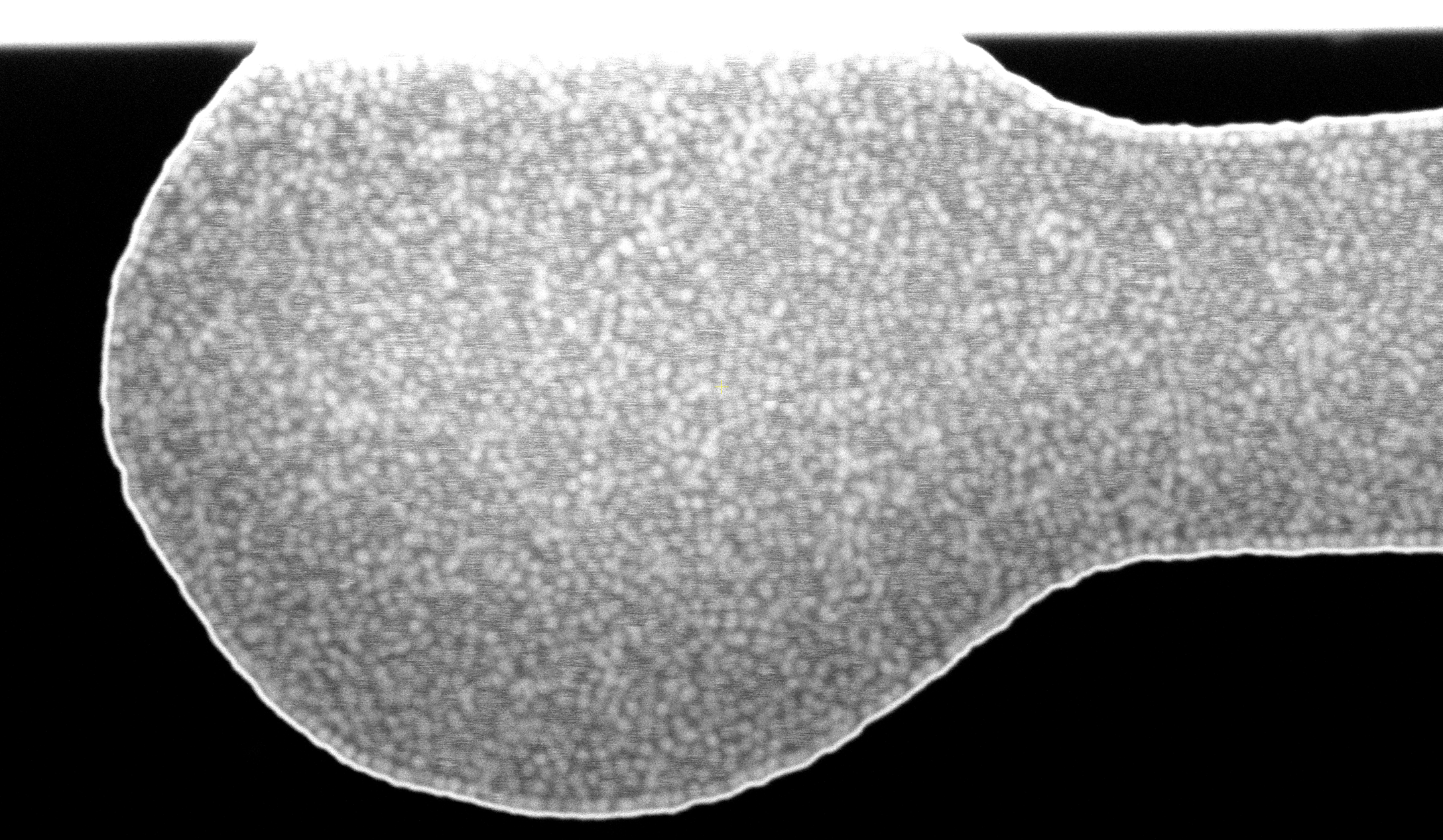
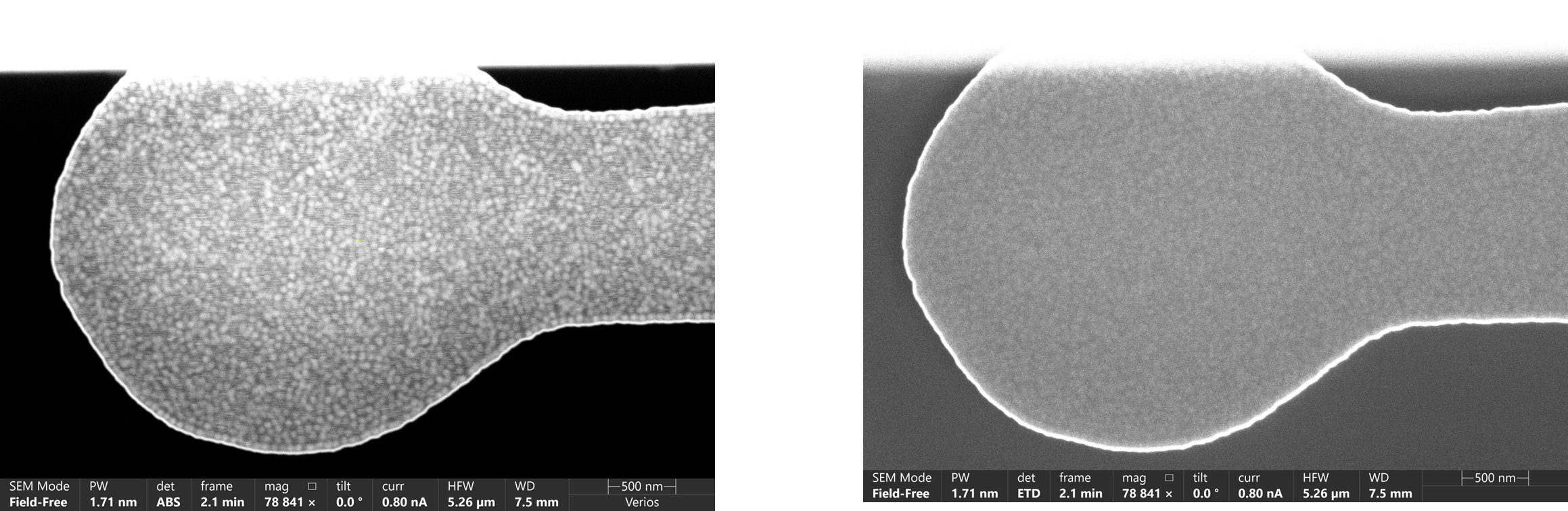
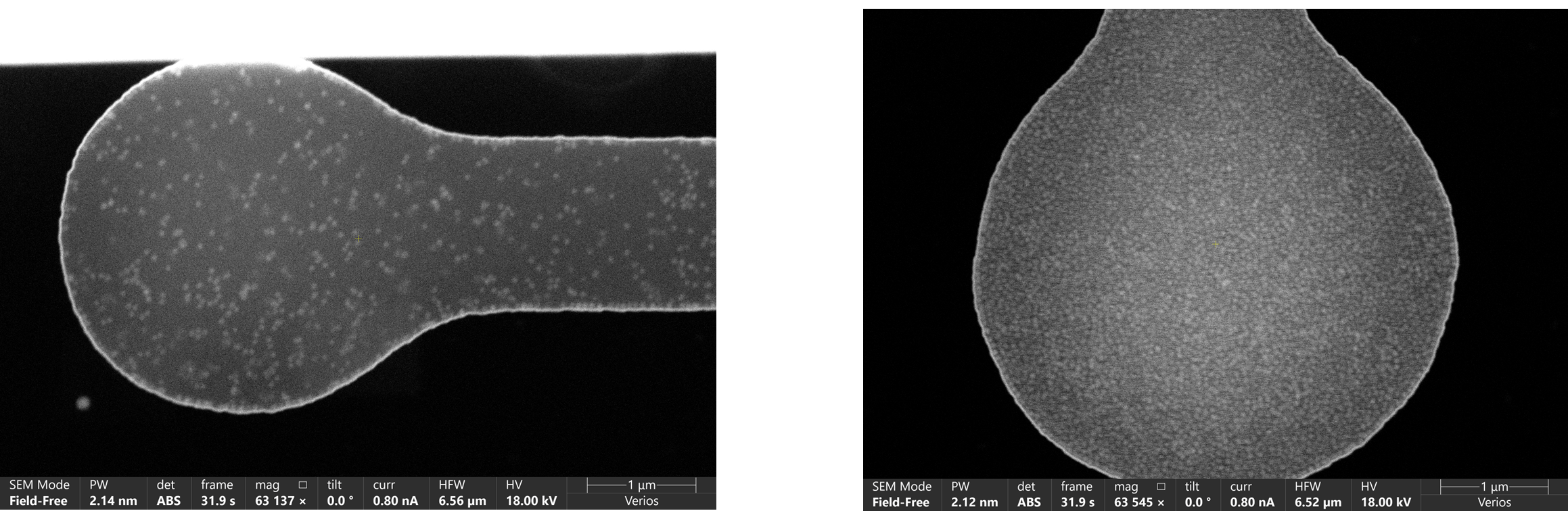
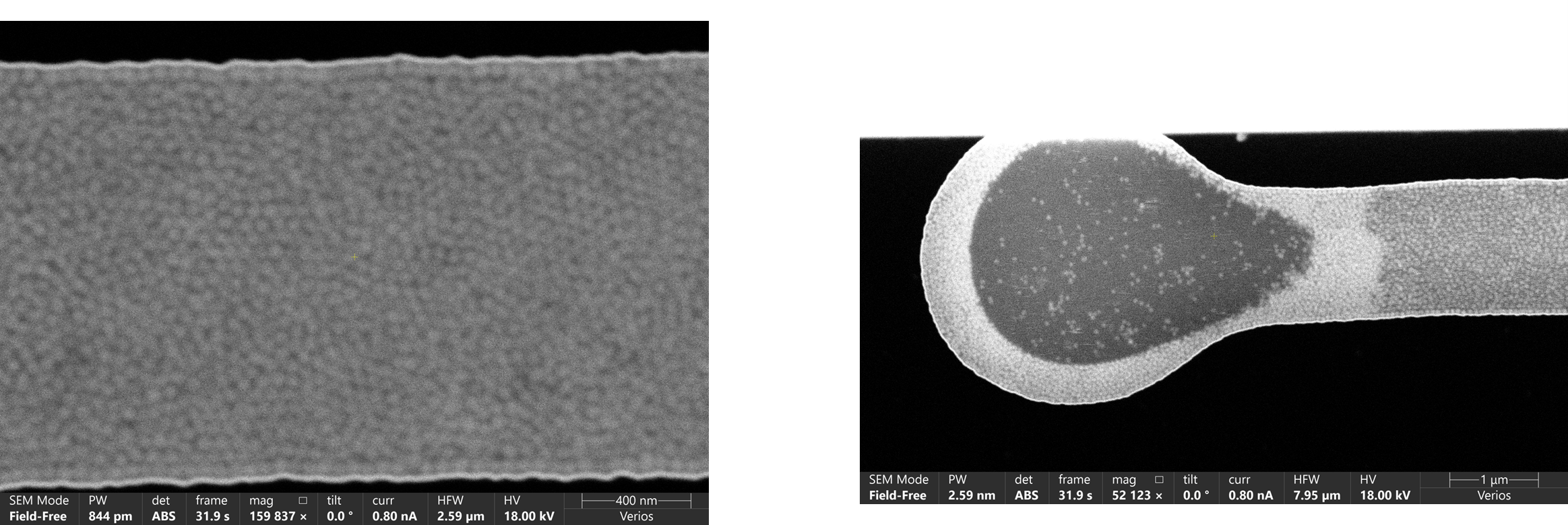
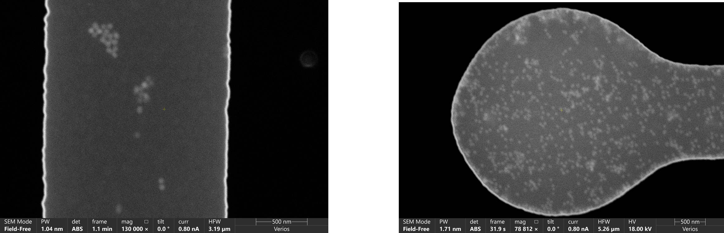
The SEM images illustrate how silica nanospheres appear in liquid, highlighting both their distribution and contrast. BSE imaging provides sufficient contrast to distinguish individual particles in liquid. The difference in signal intensity between the inside and outside of the channels confirms that the channels are filled with water. By comparison, SE imaging makes it more difficult to identify individual particles but shows the presence of liquid inside the channels more clearly. At higher concentrations, the particles are distributed in multiple layers and often overlap, which complicates distinguishing them individually. However, their movement is more restricted due to tight packing, which makes imaging easier and allows the use of slower scanning speeds. At lower concentrations, the particles are more mobile and often form small clusters.
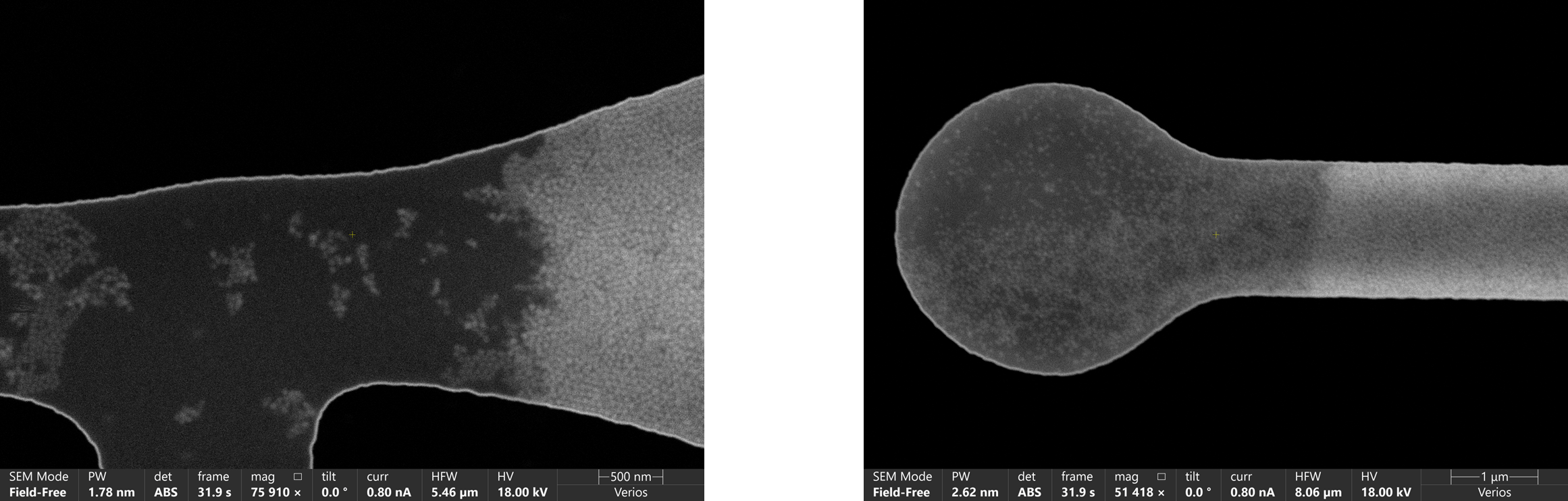
Particles at different depth layers
Observations of particles in different concentrations and in different phases of the solution
This study shows that it is possible to image silica nanospheres in liquid nanochannels using SEM with Insight Chips’ Nano Channel Chips, demonstrating their versatility for visualizing a broad range of particle types.
Chip preparation takes less than 10 minutes, enabling faster sample processing. Furthermore, the static holder design allows multiple chips or samples (up to five) to be mounted at once inside the vacuum chamber, which in turn accelerates SEM characterization.
Going forward, this imaging strategy could be extended to particles with lower atomic numbers than silica, to better define the limits of observability and contrast in liquid. This is particularly relevant for organic and pharmaceutical systems.
Beyond static imaging, Insight Chips’ SEM Flow Holder makes it possible to carry out advanced in-situ experiments such as liquid exchange, mixing processes, internal pressure modulation, and other dynamic manipulations, which open exciting opportunities for further studies.
Future work could also explore the possibility of combining of SEM with complementary techniques such as EDS to obtain a more comprehensive understanding of the samples. In addition, it would be beneficial to investigate and quantify the interactions between the electron beam, the particles, and the liquid.