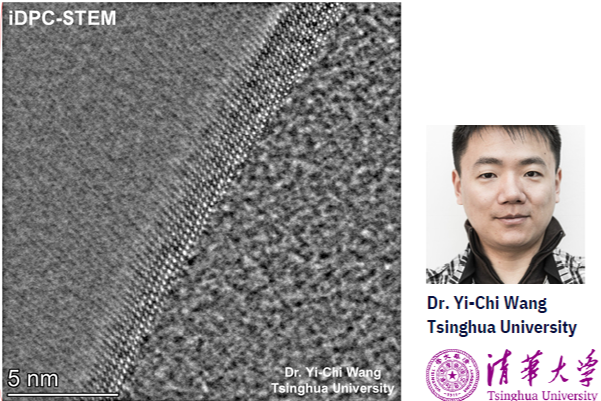
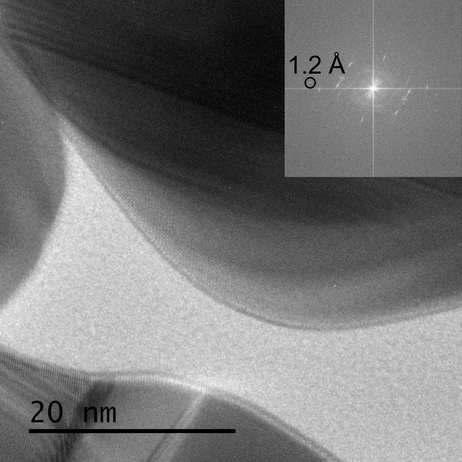
(Perhaps,in fact, the highest resolution image ever shown in a silicon nitride-basedliquid cell? Maybe... 😊)
This image is not just beautifully showing the lattices in this metal nanoparticle;it is also the first image we show taken in iDPC-STEM mode.
Itwas possible to do because the chip used contains both liquid channels of 290nm thickness, AND 50 nm thickness. The 50 nm channels precisely matched thesize of the particle, which was also about 50 nm.
Due to this ideal match, this particle was found to be held in place between thetwo 20 nm SiN membranes with no extra liquid on either top or bottom.
This offers the opportunity for superb resolution, both due to minimal excessliquid, but also due to the membranes keeping the particle fixated, eliminatingany Brownian motion that would occur if the liquid layer were just slightlythicker.
The final ingredient is, of course, an excellent TEM operator! And that ingredientwas also present in this case, as the image was taken by Dr. Yi-ChiWang fromProf. Xiao Chen's research group at Tsinghua University in Beijing, China. With10 years of experience at the TEM, the TEM was operated with perfection.
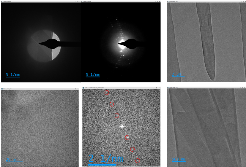
This was not a one-off image either. We were able to prepare 5 chips in a row, withall of them behaving in this way, trapping 50 nm particles in ~50 nm liquid.More images from this research group will, however, haveto waitfor the research to be published by the group itself.
For now, we attach a series of images with atomic resolution as a testimonial tothe robustness of our chips!
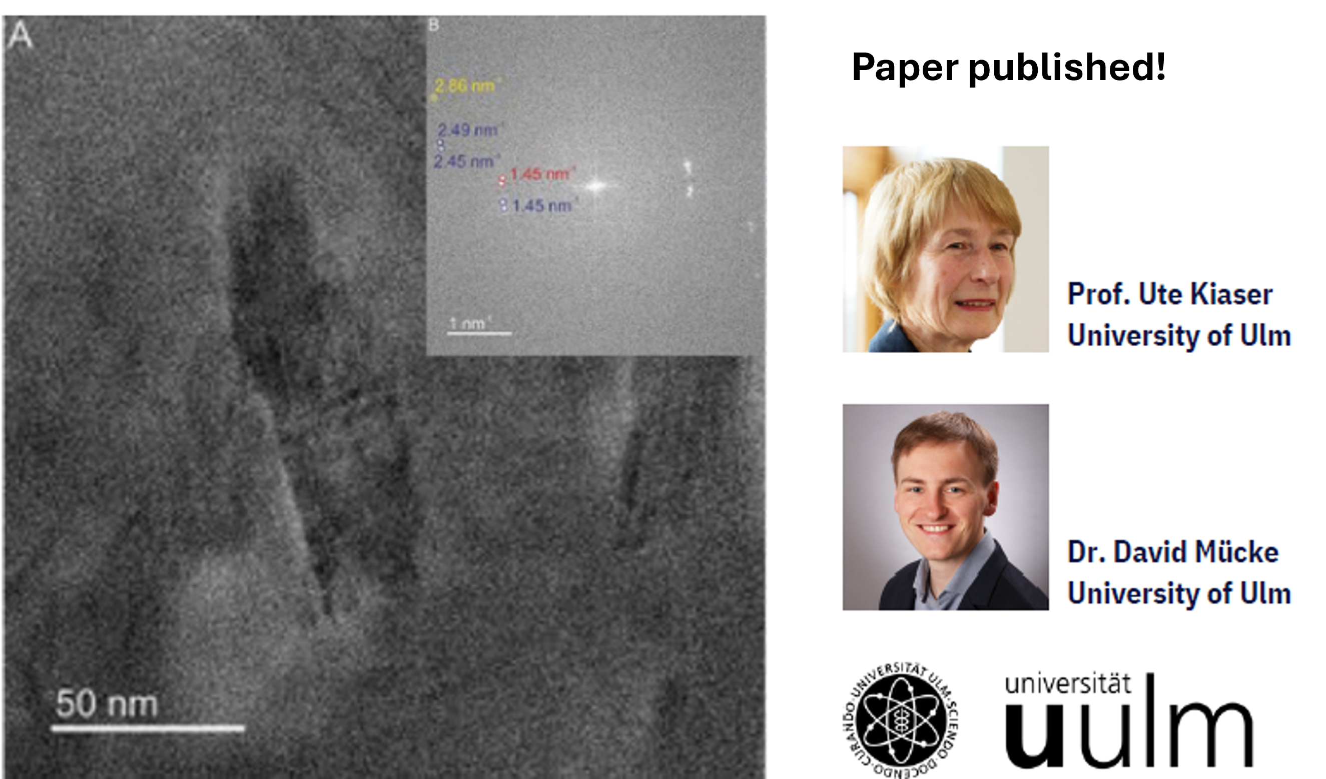
Fun fact: Prof. Kaiser's research group was Insight Chips' first ever customer!
They now managed to grow a MOF in-situ and capture it with atomic resoluion.
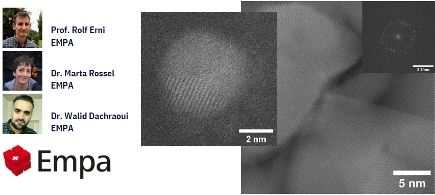
These images were captured during the first few hours at a product demo at EMPA and is a beam-induced Palladium crystal.
This result was acquired on the first try loading the Ettringite particles ino the chip. The imaging was done by Gatan applications scientist Liam Spillane, and would not have been possible to acquire with such high resolution without making the most of the impressive Gatan K3 detector.
The Ettringite is a bit special because it has to be imaged in water, as over 50% of its structure is water.
So, here you see the first-ever atomic resolution image captured of ettringite, which is a crucial component of cement.
The result was part of a paper now published with Dr. Olivia Rindle as first author.
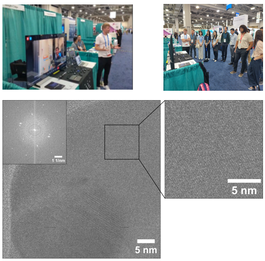
At the M&M25 conference held in Salt Lake City, we invited people to come join us for a live demo.
We had co-founder assist. Prof. Murat Yesibolati and Insight Chips engineer broadcasting live from the TEM in Denmark.
Here they took the audience through how they took a new chip, added sample solution to it, loaded it in the TEM holder, inserted the holder in the TEM - and got atomic resolution within minutes!
This whole sequence took about 20 minutes - Including 10 minutes pump time in the Titan TEM!
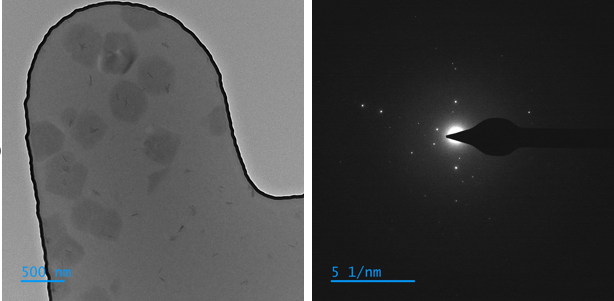
The sample seen here is silver nanoplates, imaged in 60 nm water with 17 nm SiN membranes around it.
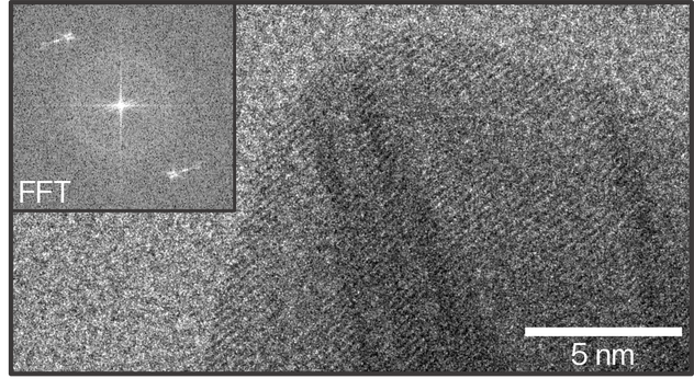
Co-founder and Assist Prof. Murat Yesibolati was able to acquire some of the most impressive images we've taken in liquid - the impressive part of this is that the liquid thickness was 500 nm, and Murat still was able to capture lattice fringes in the TEM!
ZIF-8 (with ferritin inside!) with courtesy of Joakim Lajer (DTU ) and Dr. Justin Mulvey, former PhD student in Prof. Joe Patterson's lab at UC Irvine.
This image was taken at a product demo at DTU with Prof. Xiaodong Zou from Stockholm University.
The CaCO3 crystal was grown by heating up super saturated solution inside the TEM using our (patent-pending) temperature holder!
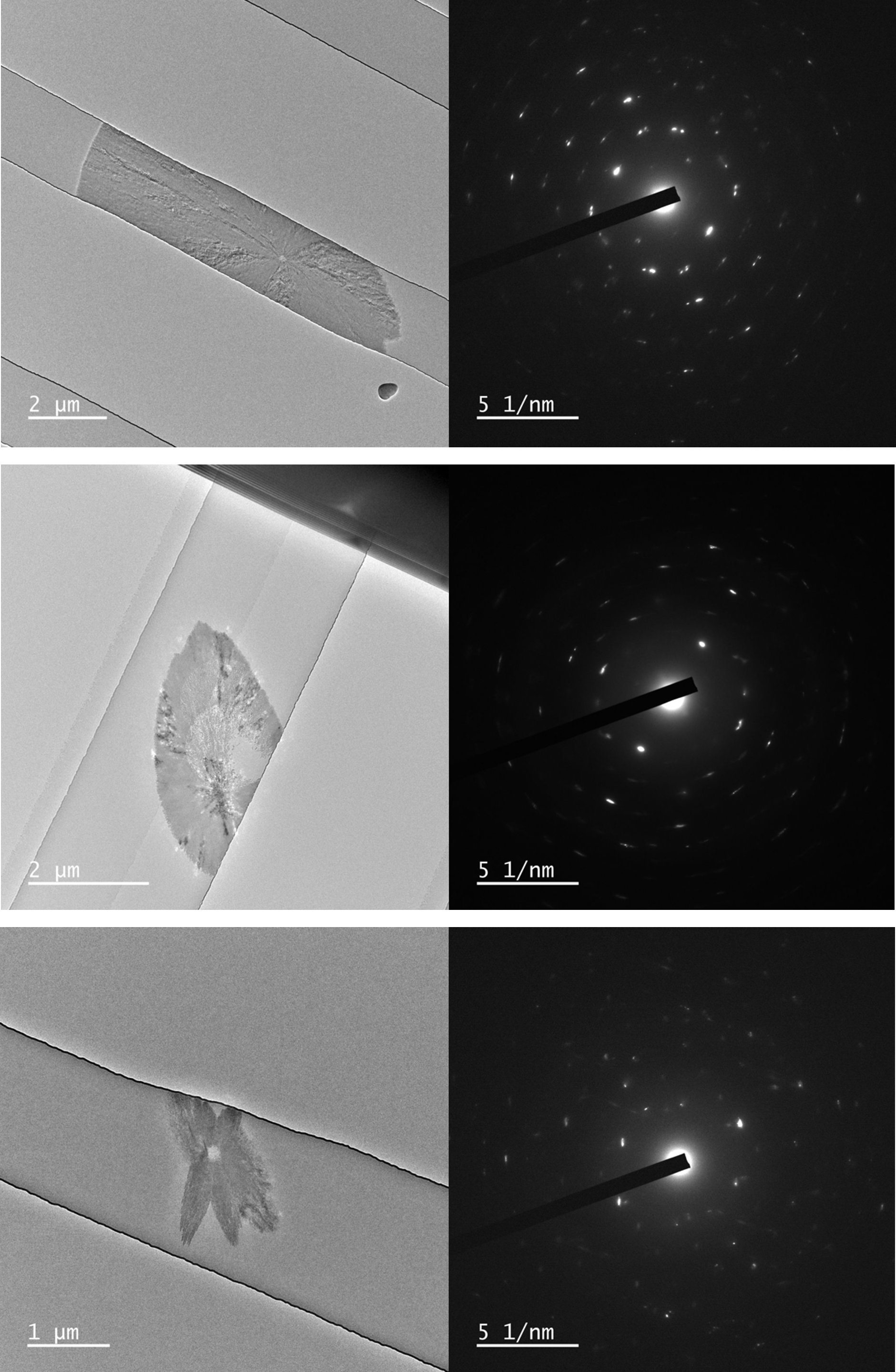
Not quite same resolution, but worth sharing again are also the amazing images taken by Dr. Tomoya Yamazaki and Prof. Yuki Kimura at the University of Hokkaido.
These images are of CaCO3 grown on their first day with the system, by mixing together 6 mM CaCl2 and 6mM NaCO3 in our chips: